Single-stage MMIC LNA for NMR
The spectrometer frequency is determined by the magnetic strength of neodymium Halbach cylinder, which in this case with B=1.038T, the nuclear magnetic resonance frequency is 44.19MHz.
Design Proposal
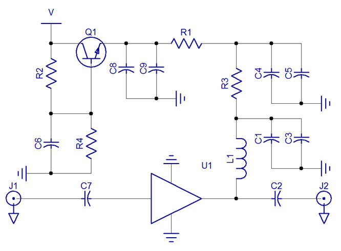
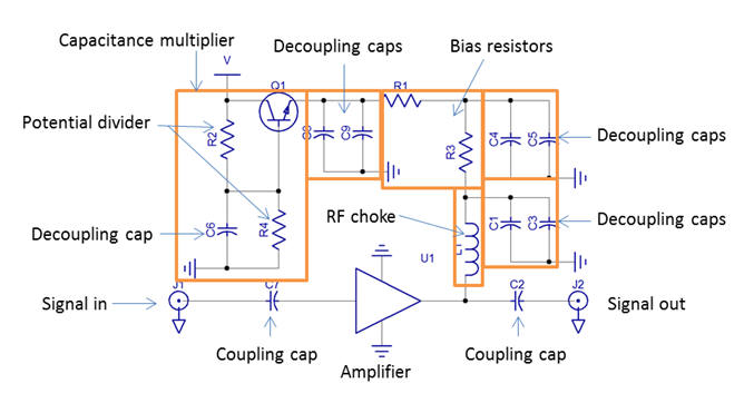
Overall the design of the low noise amplifier (LNA) circuit comprises the majority of components to support and power the amplifier itself. In the application to NMR, the signals are of extraordinarily low amplitude and so the power supply must be absolutely clean and also be capable of responding to changing current demand.
The amplifier is powered via the same pin used to carry out the amplified signal. It would be quite undesirable for the RF signal to leak back through to the power supply, and this is prevented by feeding the supply current through an inductor (L1). The inductor exploits a magnetic field to cancel out an AC signal by induction, and so the rapidly changing RF signal is blocked thereby acting as an RF choke.
The amplifier must be provided with a particular voltage and current in a very stable fashion that is free from high-load voltage-current transients. To achieve this we make extensive use of de-coupling capacitors throughout the supply line, and also a special transistor-capacitor arrangement referred to as a ‘capacitance-multiplier.’ The voltage is selected using a potential divider formed of R2 and R4 setting the transistor-base voltage, which in turn determines the transistor-emitter voltage. In this arrangement the capacitor (C6) de-coupling the transistor-base effectively has its capacitance multiplied by the transistor gain. These four components act as a large capacitor capable of compensating for variation in the supply voltage and high current transients.
The transistor Q1 outputs a voltage, and the appropriate current required by the amplifier is determined by the series bias resistance. Whilst this could be achieved using a single bias resistor, here we have split the resistance into two resistors so that we can include additional de-coupling capacitors.
When arranged in series with a signal, a capacitor can pass an AC signal and to this effect these are known as coupling capacitors. Since however the ideal capacitor comprises isolated electrode plates, these coupling capacitors do not pass DC and so can be used to prevent the passage of DC currents, isolating the various RF components.
Power supply emitter follower
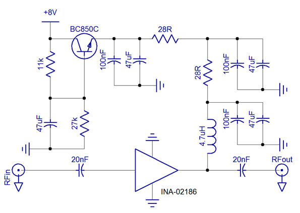
11kΩ resistor forms part of a low pass filter with C1, and if a value of 47uF is chosen, the corner frequency is significantly less than 1Hz and should hopefully provide sufficient HF noise rejection.
MMIC Amplifier
Agilent INA-02186
| NF | Gain | V (typ) | I (typ) | I (max) | RF-in power (max) | V (min) | V (max) |
| 2.0dB | 31dB | 5.5V | 33mA | 50mA | +13dBm | 4.0V | 7.0V |
The Agilent INA-02186 has a typical voltage drop of 5.5V, the typical and absolute maximum current draw of 33mA and 50mA respectively.
Bias Resistance
To provide 5.5V at 45mA from +8V then the bias network must drop 2.5V and 113mW. This is provided by a bias resistance of 55.55Ω, and is closely provided by an E24 preferred value 56Ω. This is split in two and carries the advantage of increasing de-coupling capacity. Conveniently, 28Ω 1% resistors are available.
RF-Choke
Coilcraft 1008AF-472XJLB RF chip inductor 4.7uH. This component has a DC resistance of 0.435R, and an I(rms) max of 0.65A.
According to the inductive reactance equation, `X_L=2pifL`, at 44.2MHz a reactance of 1305Ω results.
DC-Blocking Capacitor
At frequencies sufficiently below the SRF, the impedance is mainly contributed to by capacitor reactance. The reactance must be low at the operating frequency, and in practical terms, be less than 2Ω. Capacitive reactance can be calculated with the equation below.
`X_C=1/(2pifC)`
| Capacitance | Reactance |
| 20pF | 180Ω |
| 1.8nF | 2Ω |
| 20nF | 0.18Ω |