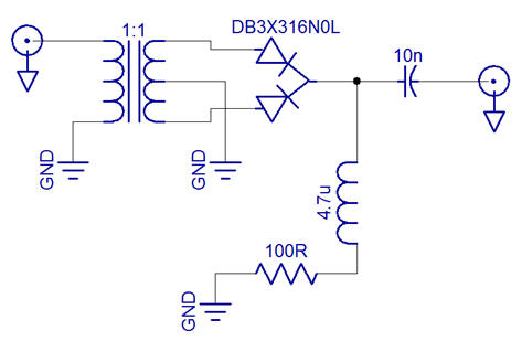
Frequency Doubler
This circuit employs a centre tapped transformer and a common cathode pair of diodes in a similar topology to a two-diode full-wave rectifier. The inductor provides a return path for the DC rectified current and the coupling capacitor blocks the DC component from escaping the device. The output is then fed to gain-block.
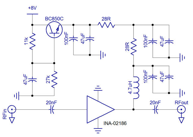
Gain block
Impedance and Drive Considerations
The initial frequency source will be provided by the AD9850 DDS and, with an output impedance of 200R, will require some form of impedance matching. To achieve this without any additional components, the 1:1 transformer is replaced with a 1:4 (is this right? The impedance transformer is a 1:2 due to sqrt(source Z / load Z) = sqrt(200/50)=2). Further, the DDS output is likely to be insufficiently high (ca. -10dB) to drive the diodes directly (required +10dB) and so will require an additional bias voltage to be applied. This can be achieved by providing the appropriate bias to the centre tap of the transformer, with a voltage clamped by an additional diode.
Filtering
The output of the frequency doubler will require some degree of filtering. The operating input frequency range will be in the region of 10-30MHz and so a filter with a corner frequency of 60MHz will be constructed. A basic Tee-filter was modelled using Micro-Cap 10.
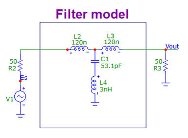
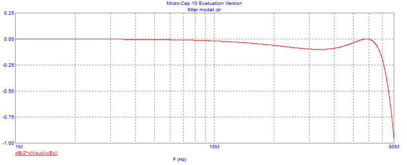
Click to zoom in.
Proposed Schematic
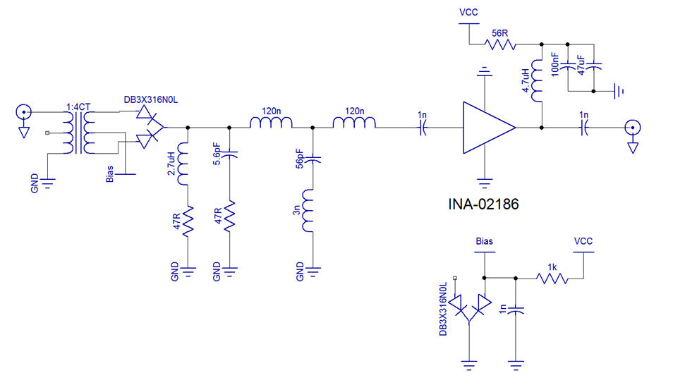
Notes
The 47 + 5.6 pF is just an experiment. Sometimes DBM and multipliers work more predictably when terminated with say 50 Ohms at harmonics (or combinations). These components help provide a near 50 Ohm termination at harmonics that would otherwise tend to infinite impedance due to the Tee LPF.
Parts List
Diodes: DB3X316N - Short reverse recovery time (0.8ns), low forward voltage.
RF-Choke: Coilcraft, 1008AF-472XJLB, RF chip inductor, 4.7 µH, 0.435R, 0.65A
Using `X_L=2pifL`, we can calculate the projected reactance offered by this inductor. Ie., This 4.7uH inductor at 22.1MHz gives 653Ω reactance.
PCB Design