Transmit-Receive Switch
The LNA must be protected from the power amp pulses.
- The passive silicon diode transmit-receive switch
- LNA voltage protection
- The active PIN diode transmit-receive switch
- Transmission line equivalent circuits
- Pi-network Inductors
- DC Bias RF choke
- Bias Driver
- Higher power PIN diode alternatives
The passive silicon diode transmit-receive switch
The RF power amplifier whilst amplifying the pulse signals will also amplify noise. This will manifest in random spikes in the RF spectrum, which becomes increasingly prevalent at lower powers until the thermal noise floor is reached. Since much of the noise spectrum is of lower power, the baseline noise figure is improved if small power signal are prevented from entering the antenna transmission line. For this purpose standard silicon rectifier diodes can be employed in series with the RFPA output. Since these diodes only begin to conduct when the input voltage exceeds the forwards voltage drop (Vf) they have the effect of blocking all signals with voltages less than this. When large power RF signal impinge the diodes, they switch on and conduct the RF current – in this respect, it is a passive transmit switch.
Since diodes only conduct the forward direction, two are required in anti-parallel arrangement. Further, since no DC bias is required for their operation, they are insulated from the antenna with an AC coupling capacitor. Once the diodes are conducting, it is necessary for them to remaining conducting until the pulses are complete and to this end, when selecting diodes, the ‘reverse recovery time’ is an important parameter to consider. For example, ultra-fast rectifying diodes including the small signal diode 1N4148 has a reverse recovery time of ca. 4ns, whereas for the standard rectifier diode 1N4007 a figure of 100us is more typical. The diodes also must be capable of carrying the full RF current, and small signal diodes are unlikely to operate without thermal runaway, the 1N4148 can carry up to 400mA, significantly short of 1Amp of a 50W signal. An important final figure of merit is the total diode capacitance, contributed by plate and lead capacitances. Whereas specialist PIN diodes have very low capacitances ie., ca. 1pF, many rectifier diodes have capacitances in the hundreds of pF range. This is a very important figure for series attached diodes, as the capacitive reactance of the diode must be low enough as to not couple the AC signal across but rather, conduct the signal through diode.
`X_c=1/(2pifC)`
| C | Xc |
| 7.19nF | 0.5R |
| 10nF | 0.35R |
| 500pF | 7.2R |
| 100pF | 36R |
| 50pF | 72R |
| 10pF | 359R |
| 5pF | 718R |
| 2.5pF | 1436R |
In summary, it is necessary to employ a diode that has a low capacitance (Ct<10pF), high repetitive reverse voltage (Vrr>200V), high forwards current capacity (IF>2A) and a reasonably high carrier life-time or reverse recovery time (trr >1us).
Satisfying these criteria, the S07M-GS08 ‘Standard recovery, high voltage’ diode was selected with Vrr=1000V, IF=1.5A (25A surge currents for 8ms), VF=1.1V and Ct=4pF.
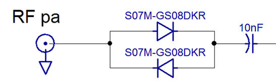
Figure: Noise blocking standard speed rectifier diodes
The capacitance of the diodes is small at 4pf, but not negligible. The two diodes in parallel afford 8pF, and this can be tuned-out by using a parallel inductor. The inductor forms a tuned circuit, which at resonance has an infinite impedance. Using the relationship below the inductor value is calculated to be 1.62uF.
`omega^2=1/(LC)`
From Coilcraft’s range of inductors, the 1008AF-152 component with a nominal inductance of 1.50uH has the actual inductance of 1.59uH. Capable of handling a forward current of 1000mA, this is significantly higher than the current which will flow since only a small RF voltage will establish across it.
LNA voltage protection
Passive protection of the LNA is also possible with standard silicon diodes. These are required to conduct harmful voltages away from the LNA input to the ground, and this can be achieved with shunt anti-parallel ‘self-biasing’ signal diodes. For this purpose, the diodes must respond very quickly to rising incident RF signals and also cease conduction rapidly. The 1N4148 small signal diode is well suited to this, have a very fast response (<4ns) and a bulk resistance of around 0.5ohm. When a rectified current flows through the diode, its capacitance increases dramatically due to stored charge and provides a low capacitive reactance path shorting the RF signal to the ground.
The forward voltage drop must be no more than the maximum LNA input voltage, which in this case for the BGA616 is 10dBm, or about 707mV, and the repetitive reverse voltage must exceed the RF power voltage. This excludes the 1N4148 diode with VF=720mV and Vrr=100V. The FID signal at around -100dB is very much smaller than the conduction voltage of even low voltage Schottky diodes and so the passive diodes cannot conduct at such low voltages and so provide little attenuation to the signal.
Schottky diodes have exceptionally low forward voltage drops (VF ca. 200mV-600mV), and very low capacitance (Ct<1pF), but they have low current capacity and inferior reverse repetitive voltage (Vrr<50V). On the other hand, Silicon-carbide Schottky diodes have very high power handling (Pdis>50W), very high current (IF>5A), very high reverse voltage (Vrr>600V), very fast response (sometimes zero recovery) but exceptionally undesirable capacitance (Ct>500pF). Whilst interesting, these SiC Schottky’s are better suited to high efficiency switching power supplies.
Although germanium diodes exhibit low voltage drops, only standard Schottky diodes really have appropriate voltage drop and current handling figures and they are used in a special arrangement with a PIN diode to form the Schottky enhanced pin limiter. The Schottky diode begins conduction rapidly at low voltage, providing the bias current path for the associated PIN diode. The PIN diode when biased conducts and enters a low series resistance state which allow large RF currents to flow thereby protecting the LNA. However, since the RF signal will exceed the reverse repetitive voltage the Schottky-PIN will require additional preceding attenuation, and since no DC bias is required they are again insulated from the antenna with an AC coupling capacitor.
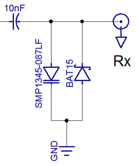
Figure: Self-rectifying PiN-Schottky pair
Here are some diodes, all with reverse recovery times (trr) less than 10ns. The BAT-15 Schottky diode with a forward voltage of 230mV, should give a limit of ~0 dBm with soft limiting. The BAV-16 etc should be OK and hard limit ~ 7 dBm. Once conducting, stored charge will reduce their impedance. The BAT15 has a maximum reverse voltage of 4V, or 25dBm into 50R.
| Part Number | Voltage Vr | Current (Io) | Voltage drop (Vf) @ If | Capacitance @ Vr |
| BAV16W | 100V | 300mA | 1.2V @ 100mA | 2pF |
| BAT15 | 4V | 110mA | 230mV @ 1mA | 0.5pF |
| BAT30F4 | 30V | 300mA | 310mV @ 10mA | - |
| BAT 60A | 10V | 3A (DC) | 370mV @ 1A | 35pF @ 5V, 1MHz |
| BAT54TA | 30V | 200mA (DC) | 400mV @ 10mA | 10pF @ 1V, 1MHz |
| TMBAT49FILM | 80V | 500mA (DC) | 420mV @ 100mA | 120pF @ 0V, 1MHz |
| BAT46 | 100V | 150mA (DC) | 450mV @ 10mA | 10pF @ 0V, 1MHz |
| BAT750TA | 40V | 750mA (DC) | 490mV @ 750mA | 25pF @ 25V, 1MHz |
| BAT1000TA | 40V | 1A | 500mV @ 1A | 175pF @ 0V, 1MHz |
| BAT30KFILM | 30V | 300mA (DC) | 530mV @ 300mA | 22pF @ 0V, 1MHz |
| BAT854W | 40V | 200mA (DC) | 550mV @ 100mA | 20pF @ 1V, 1MHz |
| BAT60JFILM | 10V | 3A (DC) | 580mV @ 1A | - |
| BAT754 | 30V | 200mA (DC) | 600mV @ 100mA | 10pF @ 1V, 1MHz |
| BAT42W | 30V | 200mA (DC) | 650mV @ 50mA | 7pF @ 1V, 1MHz |
| ACDBAT360 | 60V | 3A | 700mV @ 3A | 180pF @ 4V, 1MHz |
| BAT 165 | 40V | 750mA (DC) | 740mV @ 750mA | 12pF @ 10V, 1MHz |
| BAT 64 | 40V | 120mA | 750mV @ 100mA | 6pF @ 1V, 1MHz |
| BAT54 | 30V | 200mA | 800mV @ 100mA | 10pF @ 1V, 1MHz |
| BAT46WJ | 100V | 250mA (DC) | 850mV @ 250mA | 39pF @ 0V, 1MHz |
| BAT54WFILM | 40V | 300mA (DC) | 900mV @ 100mA | 10pF @ 1V, 1MHz |
| BAT43XV2 | 30V | 200mA | 1000mV @ 200mA | 7pF @ 1V, 1MHz |
The active PIN diode transmit-receive switch
To achieve further Tx-Rx isolation, an active PIN diode switch can be employed. PIN diodes act as current controlled resistors at RF frequencies, and when biased appropriately can change as to present either very high resistance (>10k) or very low resistance (ca. 0.5R). As such, they enable a means to control impedance match-mismatch for the transmit and receive legs of the diode switch circuit. When matching is good, the signal is free to travel through the transmission line, whereas when fully mismatched maximum signal reflection occurs. With respect to one another the two diodes are series arranged and has the advantage that only one bias choke is required, as the bias current that enables the transmit path continues through the receive diode to ground.
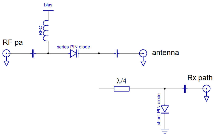
These series/shunt-diodes are placed a quarter-wavelength apart and can be achieved with a quarter length section of coax or using the equivalent circuit of a short transmission line. The quarter wave element has the effect of changing the presented diode short-circuit to an open circuit from the perspective of the transmitter and causes RF reflection rather than absorption. A PIN switch provides more than simply a controllable route to short the signal and taking into account the impedance mismatch voltage reflection, the shunt PIN diode does not carry the full RF signal power. Consequently, a pin diode can handle powers far in excess of a given thermal power dissipation rating. The advantage of Tx - series - PI - shunt Rx switching is that very little RF voltage appears across each diode. The antenna goes after the "series diode" Both diodes are forward biased for Tx
Transmission line equivalent circuits
Sometimes in RF circuitry it is necessary to use various fractional lengths of transmission line and whilst at microwave wavelengths transmission line lengths are short and can be printed onto a PCB, at lower frequencies (<100MHz) lengths can exceed 10m. To avoid the use of cumbersome lengths of coaxial cable, transmission lines can be approximated through the use of impedance matching Pi-networks. Fundamentally these Pi networks enable a convenient means to perform impedance matching, and whilst for this application the network matches 50R to 50R, they can of course match any impedance to any other ie., they can synthesise any characteristic impedance whilst coaxial cable is limited to the commercially available varieties. Whilst a transmission line of any characteristic impedance can be printed on PCB, as pointed out, lengths can be very long.
If the coax is 50 Ohms, then all components are set to j 50 Ohms reactance at f.
`C=1/(2pifZ_0)` and `L=Z_0/(2pif)`
Using these equations it is possible to calculate LC values for f=44.2MHz.
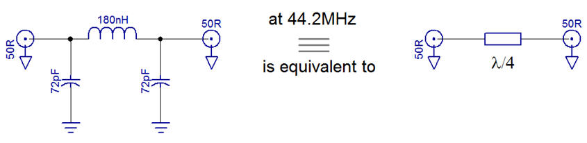
Figure: Impedance matching Pi-Network quarter-wave transformer
Pi-network Inductors
The RF current through the bias inductors will be small but the RF voltage across them is important. This causes heating as P = Vrms^2 / Rp where Rp is the parallel resistance of the bias inductor.
The bias RFC has a parallel resistance Rp = Q Xp and will generate heat.
An important parameter of inductors is their equivalent parallel resistance. This affects the degree of joule heating according to the equation below. Hence it is preferable to choose inductors with a high parallel resistance as this reduces the power dissipation proportionally. This parallel resistance varies with Quality factor and parallel reactance, and so selection should in part be guided by either Q or parallel resistance.
`P=V_(rms)^2/R_p` and `R_p=QX_p`
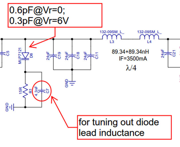
Inductance varies to a degree with frequency, and so it is important to consider this drift at operating frequency from the nominal inductor inductance. For example, consider the two components, both 180nH nominal inductance, Coilcraft 0805CS-181XGEB and Coilcraft 0603LS (1608): whilst the former has an operating inductance of 179.65nH, the latter is 180.85nH. For various other components this figure varies from 170nH to 188nH. Of those compared, the Coilcraft 0805CS-181XGEB was selected for low RF power use. However at higher powers RF current becomes quite significant and can will cause overheating and failure of inductors that are of small package. For example, 50W into 50R gives 1amp. At these currents an exact match of inductance is not possible in a single package and instead two 90nH inductors of higher current rating can be placed in series. The Coilcraft ‘Maxi Spring’ Air core inductors can handle up to 5A, and Coilcraft ‘Square Air Core Inductors’ can handle up to 5.7A but in smaller package size. The Maxi Spring 132-09SM with nominal inductance of 90mH at 44.2MHz presents 89.34mH inductance at 3.5amp in a 10.55x5.97mm2 package. At half the physical size of 5.71x5.94mm2 but with a less accurate match of inductance, the 2222SQ-90N (typical inductance 90mH, 5Amp) presents an inductance of 86.81mH at 44.2MHz. It is generally preferable to use smaller components to reduce PCB costs, and a Pi network provides a reasonably accurate quarter wave equivalent over 30% operating frequency.
The quality factor, Q is also an important parameter to consider as outlined earlier. Again this also varies with frequency, and at 44.2MHz these two inductors exhibit Q’s of 119 for the 132-09SM and 129 for the 222SQ-90N. Resultantly the power dissipations of 415mW and 394mW respectively are within the limits for these high current inductors.
| Parameters @ 44.2MHz | 132-09SM | 222SQ-90N |
| Q | 119 | 129 |
| L | 89.34nH | 86.81nH |
| Irms | 3.5A | 5A |
| DCR | 15mR | 6mR |
| Xp | 24.8R | 24.1R |
| Rp | 2951R | 3113R |
| P | 415mW | 394mW |
However since many aspects of the circuitry could lead to failure, it was decided to make use of the better inductance match of the 132-09SM 89.34mH inductor.
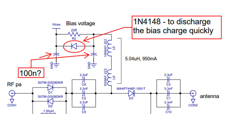
DC Bias RF choke
The bias current for the PIN diode is provided by a DC bias voltage, controlled by an associated driver circuit. The RF power signal must be prevented from propagating through the DC supply and this is achieved with an appropriate inductor RFC. For the LNA bias current, a 4.7uH inductor was selected as this provides an RF impedance of 1.3k. At high currents, with ferrite cores the eventuality of core-saturation must be avoided, as the magnetic power must be have sufficient room to compensate for RF voltages effectively. Thus high current RFC’s were investigated. There was no single inductor available that provided the desired 4.7uH at IF>300mA, but many are available in the range 1uH to 2.2uH with IF>900mA. A few of the more suitable components include Coilcraft 1008AF-192 ‘Ferrite chip’ inductor with nominal inductance 1.90uH and actual inductance 1.97uH at 44.2MHz has a current capacity of 1000mA, and from the same range, the 1008AF-222 can carry 950mA and has an actual inductance of 2.54uH.
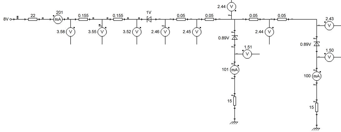
The inductors have very low resistance (<0.2ohm) and so drop very small voltages. The diodes approximately have a constant voltage drop, and the excess voltage provided from the bias must be dropped across the bias resistors. This then allow an estimation of the total series resistance required.
Bias voltage - Vf(series diode) - Vf(shunt diode) = voltage to be dropped by resistors
For example, at 5V, 5V – 1V – 0.89V = 3.11V to be dropped by resistors. The total series current is to be 200mA, and using R=V/I, 3.11V/200mA=15.5Ohm total series + shunt resistance.
Thus from the perspective of resistor selection it is preferable to have a lower bias voltage as then less excess voltage will need to be dropped by the resistors. P=I2R=V2/R
| Bias Voltage | 5V | 5V (2nd go) | 8V | 8V (2nd go) | 8V (3rd go) | 12V |
| Vdrop by resistance | 3.11V | 6.11V | 10.11V | |||
| Total series resistance | 15.5 Ω | 30.55 Ω | 50.55 Ω | |||
| Total power to dissipated | 620mW | 1.22W | 2.0W | |||
| Series Resistance | 12.5Ω | 5 Ω | 25Ω | 25 Ω | 22 Ω | 37Ω |
| Series resistor voltage drop | 2.44V | 0.97V | 4.94V | 4.74V | 4.42V | 7.42V |
| Series current | 195mA | 195mA | 197 mA | 190mA | 201mA | 200 mA |
| Series R power dissipation | 476mW | 189mW | 970mW | 900mW | 889mW | 1.48W |
| Shunt Resistance | 5 Ω | 20 Ω | 10 Ω | 12.5 Ω | 15 Ω | 25 Ω |
| Shunt current | 98.4mA | 97.7 mA | 99.2 mA | 95.2 mA | 101mA | 100 mA |
| Shunt resistor voltage drop | 0.492V | 1.95V | 0.992V | 1.19V | 1.51V | 2.51V |
| Shunt R power dissipation | 48mW | 191mW | 98mW | 113mW | 153mW | 251mW |
The first simulated circuit using a 5V bias employed a 12.5 Ω series resistance, and 5 Ω shunt resistors. This provided the appropriate current, but the series resistor dropped a rather large voltage (2.44V) and at 195mA this would result in a power dissipation of 476mW. This power dissipation is quite high and would not enable the use of typical resistors. To reduce this voltage drop a second 5V simulation employed a 5 Ω series resistance and 20 Ω shunt resistors. In this configuration the series resistor dropped 0.97V and at 195mA dissipated 189mW whilst the shunt resistance drops 1.95V and at 97.7mA dissipates 191mW. These power figures are more preferable as they enable the use of 250mW power resistors.
On second thought, since 8V is used by the amplifier and VCO circuits it has been pointed out that 8V might be more suitable. It is still generate quite a lot of waste heat, 1.22W, but due to the duty cycle it is likely that lower spec’d resistors may not necessarily fail. The 25Ω series bias resistor has to dissipate ca. 900mW, significantly beyond the handling ability of common resistors. However it is possible to group in series and parallel combination of resistors to achieve a larger power handling. On this theme, the shunt resistor value if changed from 10 Ω to 12.5 Ω, then a parallel combination of standard 50 Ω resistors can be used. 50 Ω resistors are however very expensive (pounds per unit)!
Finally, a third revision of the 8V bias simulation gave the following combination: a series resistance of 22Ω carrying 201mA drops 4.42V and dissipates 889mW; a shunt resistance of 15Ω carrying 101mA drops 1.51V dissipating 151mW. Components satisfying these specifications are available and comparatively cheaply, for example, the Panasonic ERJ1TNF22R0U is a 1W, 22Ω, 1% tolerance, 200V thick film resistor in a 2512 imperial package, costing £0.16/unit; and the Vishay Draloric CRCW12065R0FKEA is a 250mW, 15Ω, 1%, 200V thick film resistor in 1206 imperial package, costing £0.23/unit.
Bias Driver
In order to ensure the bias current is pinched off quickly as to mute the primary Tx PiN diode rapidly, we employ an NPN-PNP transistor pair which either sources or sinks the supply current. The PiN diode retains charge when turned off and it is necessary to provide this charge a low-impedance route to the ground. In the ‘on’ state, the control circuitry (FPGA/microprocessor) sources current from the positive rail via the PNP transistor, which proceeds through the bias resistor and RF chokes. In the ‘off’ state, the PNP transistor turns off and the NPN transistor turns on which provides a return path for stored charge to the ground. An extra diode is introduced anti-parallel to the bias resistor, which means the stored charge can flow un-resisted backwards through the bias circuitry rapidly to the ground. For this application a general purpose diode is used, the DA22F2100L. As is typical, 10nF de-coupling capacitors are employed to buffer changing current demand, which, too, are discharged through the reverse bias diode.
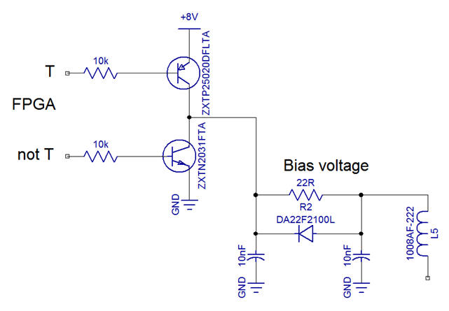
The transistors must be quick to act, both turning on with little delay, and also turning off rapidly without a prolonged delay. Additionally, the transistors must be able to handle a moderate current demand. Satisfying these criteria, the medium power NPN transistor by Zetex Semiconductors, ZXTN2031FTA and the PNP transistor, ZXTP25020DFLTA were selected.
| ZXTP25020DFLTA [PNP] | ZXTN2031F [NPN] | |
| IC(cont) | 1.5A | 5A |
| VCE(sat) | 85mV @ 1A | 40mV |
| RCE(sat) | 54mR | 24mR |
| PD | 350mW | 1.2V |
| fT | 290MHz | 125MHz |
| td delay time | 14.2ns | 16ns |
| tr rise time | 16.3ns | 27ns |
| ts storage time | 186ns | 468ns |
| tf fall time | 32.7ns | 44ns |
Higher power PIN diode alternatives
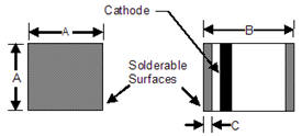
It may desirable in the future to upgrade the NMR system to accommodate a higher power exciter. The MACOM series diode, MA4P7446 can handle incident powers of 57dBm (ca. 500W). An alternative to this diode could be the Cobham Metelics / Aeroflex MMP7079-127-4. Conveniently, the Aeroflex case style CS127-4 (0.181x) is of very similar dimensions to the MACOM case style ‘1091 MELF,’ and thus should be interchangeable on the pcb.
| MACOM 1091 MELF | Aeroflex CS127-4 |
 |
  |
| A = 0.138" B = 0.180" C = 0.008" |
A = 0.143" B = 0.181" C = 0.016" |
The LNA then also needs protection from higher powers. These shunt diodes must have very short carrier life-times such that they revert to their high resistance state rapidly once the exciter is muted. To this effect, the Skyworks SMP1345-087LF has a carrier life-time of 100ns, and can reflect powers up to 40W CW (400W pulse). In the current 50W design, each of the three shunt stages employ the SMP1345-087LF (Vf=890mV, <1R, 100ns, 200mA, 0.5W). Provided the first stage has a flat leakage power that can be adequately handled by the next, to accommodate higher powers the design need not replace all of these. The Cobham Metelics / Aeroflex PIN diode, MLP7121 is quick with a life-time of 50ns and can handle input powers of up to 63dBm (or nearly 2kW!), with flat leakage of 41dBm (12.6W or 25V into 50R). The Skyworks diode can accommodate this leakage power (upto 46dBm), with the datasheet quoting 40W, or 46dBm and so only the first of the stages needs to be replaced.
Whereas the Skyworks diode is in a QFN (2x2mm) package, the Aeroflex diode is in a SOD-323 package. The case sizes are not drastically different, but one of the pads requires enlarging.
 |
Skyworks SMP1345-087LF QFN 2x2mm |
 |
Cobham Metelics / Aeroflex SOD-323 |
 |
Overlay of the two |
More stuff