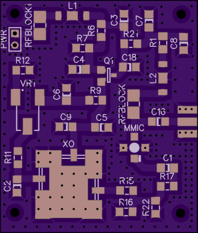
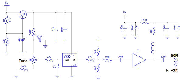
VCO
The spectrometer frequency is determined by the magnetic strength of neodymium Halbach cylinder, which in this case with B=1.038T, the nuclear magnetic resonance frequency is 44.19MHz. As to facilitate down-mixing to the audio range, the spectrometer will be purposefully mis-tuned from the NMR frequency by ca. 20kHz. The precise NMR frequency depends on several factors including temperature and pressure, but in particular, the application of any shim-fields used to correct permanent-magnet field-inhomogeneity. In this respect, it is highly desirable for the oscillator to be tuneable.
It remains to seen whether the tuning voltage can be controlled in a manner precise enough to obtain the desired frequency resolution.
The main signal source is a Z-Comm V044ME01 VCO. This has a set frequency range of 42-46MHz and accepts a tuning voltage of between 0.5 and 4.5V. It runs between 5V and ground, and is quoted to typically draw 8mA (5V/8mA=625ohm, does VCC need a resistor?). It has an input capacitance of 500pF max (whats the significance of this?). The VCO has an output impedance of 50Ω and requires isolation from devices that may cause adverse loading and impedance mismatch. The use of an attenuator and amplifier can provide this isolation. The VCO is designed to operate with an output VSWR (whats this?) of less than 1.67:1 (RL=12dB). The oscillator supply and tuning voltages must be free from any spurious high frequency noise as these will degrade VCO function. A tuning voltage loop filter and supply emitter follower are recommended in the datasheet.
|
Z-Comm V044ME01 Voltage Controlled Oscillator |
|
|
Frequency Range |
42 – 46 MHz |
|
Phase noise |
-118 dBc/Hz |
|
Harmonic Suppression |
-13 dBc |
|
Tuning Voltage |
0.5 – 4.5 V |
|
Tuning Sensitivity |
3 MHz/V |
|
Power output |
-1 ± 2dBm |
|
Impedance |
50Ω |
|
Input Capacitance (max) |
500pF |
|
Pushing |
<1 MHz/V |
|
Pulling (14dB return loss) |
<1 MHz |
|
Supply Voltage (nom) |
5V |
|
Supply Current (typ) |
8mA |
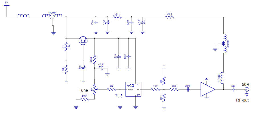
VCO supply
To achieve voltage stability from the supply rail, a transistor capacitance multiplier circuit is proposed. A low-pass filter comprising R1 and C1 rejects ripple by a factor increased by the gain of the transistor. During voltage supply transients, the capacitor responds with a movement of charge as to maintain the base current, which in turn allows for a proportional change in collector-emitter current.
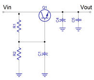
R1 also forms part of a potential divider along with R2 providing the follower voltage reference for the transistors emitter stage. Whilst the VCO requires 5V, the MMIC operates more efficiently with a higher bias voltage. It was felt that 8V was a reasonable compromise between low power dissipation, good performance and availability of resistors for the potential dividers that give the required voltage. For this purpose with R1=11kΩ and R2=27kΩ, approximately 5.7V (5.684V) is obtained for the transistor bias point and it may be possible to adjust the supply voltage slightly around 8V to achieve exactly 5V between the emitter and ground once the transistor voltage drop is subtracted.
This 11kΩ resistor forms part of a low pass filter with C1, and if a value of 47uF is chosen, the corner frequency is significantly less than 1Hz and so will provide amble HF noise rejection.
Tuning Voltage Loop filter
A clean voltage of between 0.5 and 4.5V is required to frequency tune the VCO, and for reliable operation must be free from noise. With the exception of during controlled frequency ramps, a highly stable, DC tuning-voltage is required. Thus AC signal rejection is achieved with low-pass filters, and voltage selection achieved with a potential divider. De-coupling of the VCO RF signals must be achieved at all ports of the VCO.
The basic RC low-pass filter provides a low impedance path for high frequency signals to the ground via shunt capacitors, and to increase the frequency roll-off and rejection an extra stage is added. The filters must be designed to remove 50Hz mains hum and also RF coupling from the VCO which may be expected at around 44MHz. For the basic RC filter, each the corner frequency is found with the following equation.
`f_c=1/(2piRC)`
It is also necessary for the low pass filter to permit manual tuning in a responsive manner and so the time constant RC must reasonable small, for example <100mS. This means that the values of R and C must satisfy the corner frequency and time-constant simultaneously and places restrictions on which resistors and capacitors can be used.
Tuning voltage is obtained via variable resistor VR1 which could perhaps be implemented as a digital potentiometer. To scale the input voltage of 5V to the appropriate range, that is 5V±10%, the sum of resistances R1+R3 must equal 20% that of the potential divider comprising R1, R3 and VR1. Ie., a variable resistor with resistance exactly four-fold greater than R1+R3 is required. Also, R1 forms part of the first low pass filter for which there is a practical maximum capacitance available in this design. 47uF capacitance is towards the upper end of affordable SMD capacitors.
With a 47uF capacitor, a 500ohm resistor produces a corner frequency of 6.8Hz and a time-constant of 24ms. Conveniently, 4kohm variable resistor is available to provide the exact potential division.
Current to the second low pass filter must flow through all preceding resistors. To limit the effect of adjusting the variable resistor on the performance of LPF2, it is preferable for the RC resistance to be much larger than the resistance that preceded it. For example, with the 500R and 4k variable, the resistance can vary from 500R to 4500R on top of the LPF resistance. Choosing a value for R2 of 47kohm keeps this variation low, and when in combination with a 1uF capacitor provides a corner frequency of between 3.4Hz and 3Hz and a time-constant of between 47ms and 52ms.
Isolation
Depending upon the choice of amplifier, the attenuator pad can take one or more forms. For example, an unbalanced attenuator such as the L-Pad comprising one series and one shunt resistor, or an impedance balanced equivalent such as the T-pad and the Pi-pad.
The amplifier itself could perhaps be a RF transistor based circuit (ie., MPSH10). The advantages of a transistor based design are ease of construction (no surface mount components) and also no need to balance the attenuator due to high input impedance. Alternatively an off-the-shelf amplifier block such as one of Minicircuits offerings guarantees a level of performance but has also a defined and balanced impedance. Much of the circuit design is simplified using one of these MMIC amplifier blocks and also matches the impedance of the VCO, an MMIC is the sensible choice.
Attenuation
Choice of attenuator is limited to those impedance-balanced at 50Ω. The other common alternative is the T-pad attenuator. Since we are interested in 50Ω designs, the two series resistors are of equal resistance.
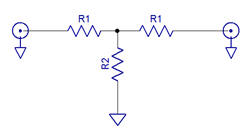
The values of R1 and R2 can be calculated with the following equations, but first the impedance factor (K) must be found. The impedance factor (K) can be calculated from the Attenuation, A.
`K=10^(A/20)`
Thus to achieve a 10db attenuation, K = 3.16. Then the following equations relate resistances to impedance and impedance factor.
`R_1=Z(K-1)/(K+1)` and `R_2=2ZK/(K^2-1)`
These give the resistance of the series resistor to be 25.96Ω and that of the shunt, 35.17Ω, which to a reasonable approximation is 27Ω and 34Ω (parallel 68Ω).
Amplifier
Minicircuits, Agilent, and others produce a large array of balanced MMICs. In this case the MMIC does not need to be especially sensitive as the signal from the VCO is not weak, and does not need to possess an especially large gain to perform its buffering role.
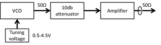
A variety of MMICs are powered through the RF-out port and so the DC offset voltage must be kept local to the MMIC through the use of DC-blocking capacitors, with a reactance low enough as to prevent interference with genuine RF signals, on both RF input and output.
A by-pass capacitor must also be used to prevent stray coupling to or from other devices connecting to the Vcc rail, and further a series RF choke is required to pass only supply current.
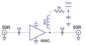
To avoid adverse effects on supply current due to variation in supply voltage, a series resistance is required between the amplifier and the supply voltage. The series resistance approximates a constant current source, and one is selected as to provide the maximum current draw. For this reason it is preferable to use a large bias resistance, which in turn requires a large supply voltage. Further it is desirable for ample de-coupling of the MMIC.
Comparison of Amplifier Components
|
|
Agilent INA-02186 |
MCL Gali-4+ |
MCL Mar-6SM |
MCL Mav-11SM |
|
Range |
DC – 0.8GHz |
DC – 4GHz |
DC – 2GHz |
0.05GHz – 1GHz |
|
Noise Figure |
2.0dB @ 0.5GHz |
4.0dB |
2.3dB |
3.6dBm |
|
Gain |
31dB @ 0.5GHz |
14.4dB @ 0.1GHz |
21.8dB @ 0.1GHz |
12.7dB @ 0.1GHz |
|
Voltage (typ) |
5.5V |
4.6V |
3.5V |
5.5V |
|
Current (typ) |
33mA |
65mA |
16mA |
60mA |
|
Current (max) |
50mA |
85mA |
50mA |
80mA |
|
RF-in power (max) |
+13dBm |
+20dBm |
+20dBm |
+13dBm |
|
Voltage (min) |
4.0V |
4.2V |
- |
- |
|
Voltage (max) |
7.0V |
5.5V |
- |
- |
The Agilent INA-02186 has a typical voltage drop of 5.5V, the typical and absolute maximum current draw of 33mA and 50mA respectively.
De-coupling
Tantalum electrolytic capacitors are common for use in surface mount applications where high capacitance but small size is paramount and are available exceeding 47uF. They are not constructed as a roll like those of aluminium construction and so are largely free of parasitic inductance but like the aluminium capacitors possess high effective series resistance. This last feature means in practical terms, parallel capacitors are unlikely to form detrimental resonances together, an advantage of this arrangement being the provision of a low impedance path for both HF and LF noise. So it is possible to use a large capacitance 47uF tantalum de-coupling capacitor in parallel with a smaller 100nF ceramic disc for added noise rejection.
Bias Resistance
The bias resistor must be selected as to prevent the MMIC from drawing excessive and damaging currents from the power-supply. This resistor will be required to drop the remaining supply voltage, once the MMIC voltage has been subtracted. From 8V this leaves 2.5V, and if the current is limited to a figure of 45mA, then the maximum power dissipation is 113mW which means a standard 125mW resistor should suffice. This would require a bias resistance of 55.55Ω, and is closely provided by an E24 preferred value 56Ω. Even at the lowest resistance for a 1% tolerance (55.46Ω) there is no chance of exceeding the MMIC absolute maximum rating or the power rating on a 125mW resistor.
An alternative approach and one perhaps superior, involves splitting the bias resistor in two and this carries the advantage of increasing the extent of de-coupling. Conveniently, 28Ω 1% resistors are available.
Bias Tee and RF-Choke
To prevent RF signals leaking through the supply rail via the bias current, a series RF-choke is introduced. The inductor itself should have a low DC-resistance and a sufficient DC-power capacity. To effectively block RF signals, an inductor is required with a large reactance at the RF frequency. In general the RF choke reactance should exceed 500Ω – ten times higher than the characteristic impedance at the operating frequency, however this rule is not always appropriate. The reactance is calculated with the equation below.
`X_L=2pifL`
For the 44MHz signal, an inductor of 1.81uH provides 500Ω reactance. Inductors of large inductance are un-economical and bulky and so it is preferable to use those of smaller values, although values up to 470uH are common (for which a 44MHz signal would be presented with a 130kΩ reactance).
Alternatively a choke can be selected according to its self-resonant frequency. At this frequency the inductor has its greatest reactance and forms a simple one-element first order filter.
The commercially available 30uH B82134 Series inductor by Epcos, has a significantly higher current rating at 1.5A than required (100mA) but has the SRF of 44MHz. This has a DC-resistance of 0.30Ω and in combination with the bias resistance gives 56.3Ω and so will not significantly affect the MMIC bias current.
If the system were to suffer a power supply failure then the bias current would drop, causing an emf to be generated by the inductor as the magnetic flux decays. It may be necessary to protect the MMIC from any harmful reverse emfs. With an 8V supply, the bias series resistance of 56.3Ω drops 2.5V when supplying a current of 45mA to the MMIC. The voltage drop across the inductor is minimal (0.3Ω /56.3Ω), and the current is low.
`"emf"=L(dI)/(dt)`
Coilcraft 1008AF-472XJLB, RF chip inductor, 4.7 µH
R=0.435R and Irms=0.65A
DC-Blocking Capacitor
The requirement for the DC-blocking capacitor is to contain the bias voltage provided to a stretch of the circuit by presenting a large DC-resistance whilst passing high frequency RF signals by presenting a low RF-reactance. A capacitor may be selected based on its Series Resonant Frequency (SRF). A capacitor has its minimum reactance at the SRF, and is therefore also acting like a band-pass filter. At the SRF, the impedance is equal to the ESR, and whilst these values are generally quite low they will contribute towards un-balancing the impedance.
At frequencies sufficiently below the SRF, the impedance is mainly contributed to by capacitor reactance. The reactance must be low at the operating frequency, and in practical terms, be less than 2Ω. Capacitive reactance can be calculated with the equation below.
`X_c=1/(2pifC)`
We note that the frequency of interest is at ca. 44MHz.
| Capacitance | Reactance |
| 20pF | 180Ω |
| 1.8nF | 2Ω |
| 20nF | 0.18Ω |
| 20uF | 1.8x10⁻⁴Ω |
The above table suggests that capacitances in the order of picofarads result in very high reactance, and that capacitances larger 1.8nF yield reactances below the threshold of 2 Ω. Tens of nanofarads provide reactances less than one ohm, but larger capacitors rely on different capacitor technologies that have significantly higher effective series resistances that would contribute to impedance mismatch. Ceramic and plastic dielectric capacitors (see table in next section “Capacitor Technologies”) have very low effective series resistance (<0.02 Ω) and are available in the nanofarad range and seem a sensible choice with a value of 20nF.
Design Proposal #1
Design Proposal #2
Component List
| What | Hmmmm | Quantity |
Manufacturer |
Description |
| Buffer amplifier | 1 |
Agilent |
MMIC 31dB gain, 2db NF, DC-0.8GHz |
|
| VCO | 1 |
Z-Comm |
42-46MHz VCO |
|
| Cap multiplier | BC850C | 1 | nexperia | SOT23, General purpose NPN |
| Noise suppression | nfe61pt472c1h9 | 2 | Murata | |
| Resistors | 11k | 1 | Vishay | 1206 |
| 27k | 1 | Vishay | 1206 | |
| 47k | 1 | Vishay | 1206 | |
| 499R | 2 | Vishay | 1206 | |
| 28R | 4 | Vishay | 1206 | |
| 68R | 2 | Vishay | 1206 | |
| Capacitors | 100nF | 3 | Murata | 1206 MLCC ceramic cap |
| 1uF | 1 | Murata | 1206 MLCC ceramic | |
| 22nF | 2 | Murata | 1206 MLCC ceramic | |
| 47uF | 5 | Murata | 1206 tantalum | |
| SMD potentiometer | 5k pot | 1 | Bournes | SMD single turn trimmer 5K 10% top adj |
Comparison of Capacitor Technology
|
Dielectric |
Body |
Inductance (nH) |
Resistance (ohm) |
|
Ceramic |
SMD |
2 |
0.02 |
|
|
Radial |
6 |
0.07-0.15 |
|
|
Axial |
12 |
0.07-0.15 |
|
Plastic |
SMD |
2 |
0.03 |
|
|
Radial |
5+ |
0.01+ |
|
|
Axial |
12+ |
0.01+ |
|
Aluminium |
SMD |
13 |
9.0 |
|
|
Radial |
15+ |
1.5+ |
|
|
Axial |
20 |
1.5+ |
|
Tantalum |
SMD |
- |
3.0 |
|
|
Radial |
10+ |
1.0 |
|
|
Axial |
15+ |
1.0 |
According to Walter G. Jung and Richard Marsh
"Up to values of about 10,000 pF, polystyrene is the best all around choice, as it has reasonable size and is readily available in many sizes, with tight tolerances available. Above 10,000 pF, and up to 0.1 u F, it still can be used but is much harder to obtain. Above, 0.1- u F polypropylene (or metalized polypropylene) is the dielectric of choice, as it has nearly the same relative qualities of DF and DA as polystyrene. Tight tolerances are available (but will be special order), and you can get capacitors up to 10 u F or more."
Moving Forwards
Not all component values were found to be available, and so some of the values were approximated. For example, the RF-coupling capacitors 20nF were replaced with 22nF, cheap and available. Also I found some "T-type circuit EMI suppression filters" in the components box, and so for added noise rejection these were used to filter the 8V supply and another to isolate the RF-side circuit from the DC supply.
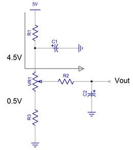
PCB Design and Fabrication
To design the PCB and sketch the circuit diagram, Diptrace was used, which is free to use. A double-sided PCB was pursued such that the top-side was used for signal routing whilst the bottom-side constituted a continuous ground plane, which is important to prevent RF interference. For PCB manufacture, I stick to the American hobbyist PCB manufacturer, OSH-Park - PCB by the square inch, $5. The design cost $16.65 for three boards.