Contents
- Design Drivers for an X-Band Receiver?
- Determining Suitable Specification Targets
- Component Selections and Preferred Suppliers
- PCB Substrate Selection
- Architectures
- Summary
- Future Articles
Design Drivers For A X-Band Receiver?
In part 1 we estimated that a Martian satellite transmitting 20 watts would create a signal to noise ratio (SNR) of 34.1 dB / 1Hz on Earth assuming the use of two 3 meter dish antennas and at closest approach (78.9 Gm). Could a low cost receiver be designed to intercept these signals?
Prior to design, it is useful to identify a few key design drivers. For example, in weak signal environments, strong overload immunity will be relatively unimportant whereas achieving a low noise figure have high However, amateur radio enthusiasts do not have unlimited finance so costs are also important. Further, designs that require multiple tuning adjustments may require expensive test equipment and reducing or eliminating these may also be desirable.
Listing a few key drivers can be useful prior to defining specifications as this provides an objective method for selecting between various implementations. It is common to identify many candidate design approaches that will all satisfy design objectives but some will better match design drivers than others. Therefore listing some key design drivers that identify what a designer is actually trying to achieve can be useful.
Some key drivers include low noise noise figure (NF < 2 dB), reasonably low cost, minimal tuning adjustments, use of modern high performance SMD components, and simple construction. The project should also be education and introduce readers to design concepts that will be useful in other receiver design projects. These goals set a scene for general design objectives, however can such receivers systems, consistent with these design drivers be realised?
Determining Suitable Specification Targets
Having identified some key drivers, defining some specification targets is appropriate. Since satellites orbiting Mars transmit signals between 8.4 and 8.5 GHz, this identifies a suitable RF frequency range. Also some commercial receivers and “USB dongles” can process signals up to 1.3 GHz, setting an IF range from 1.2 to 1.3 GHz also seems sensible. Using a moderately high IF also allows the use of very low cost, fixed image rejection filters as opposed to tuned helical filters. This design decision is compatible with previous key design drivers.
The receiver noise figure (NF) on FR4 substrates will not be as low as NF ~ 0.3 dB but setting NF < 2dB represents a reasonable goal. This is consistent with low substrate cost and allows the use of inexpensive silicon bipolar (SiGe) for RF LNA. For example, Infineon's BFP840FESD device has FT ~ 85GHz and can be obtained from Digikey (NZ) for as little as $8.13 total for 10 units. These have an advantage over HEMT (FET) devices as they operate in 50 Ohm systems and avoid any need for high Q matching networks. Typical NF~1dB at 8.5 GHz.
MMIC “gain blocks” have become increasingly popular and the LEE-39 from Minicircuits offers 13.5 dB power gain at 8.5 GHz, combined with a low NF~2.4 dB. Its gain increases to 21 dB at 1.3 GHz so it is well suited for second LNA application, post mixer gain and LO buffers. It is also inexpensive at $US1.19 each for 20 units. If we assume the SiGe LNA1 followed by a MMIC LNA2, ~12 dB mixer loss and a MMIC post mixer amplifier, conversion gain will be Gc ~ 15 + 13.5 – 12 + 21 = 37.5 dB.
The system will be locked to a 10 MHz reference, either a OCXO, GPS system or lower cost TCXO. Signals from Mars may have significant Doppler shifts so exceptional frequency stability may represent an overkill. However we will specify that the X-band receiver will operate from a 10 MHz reference, regardless of its source.
Finally, the supply voltage can be determined. Most SiGe devices only require a few volts to operate, MMIC devices usually operate from a supply of +8V with simple resistive bias and typical VCO modules only require +5V. Consequently, the X-band receiver can be expected to operate from a single +8V supply. This can be derived from a higher +12 V input using a simple linear regulator if required.
Specification Summary
| RF Input Range | 8.4 to 8.5 GHz |
| IF Output Range | 1.2 to 1.3 GHz |
| Conversion Gain | 37.5 dB, approximate |
| Reference Frequency | 10 MHz |
| Supply Voltage | +8 V, internal regulation assumed |
The current budget will now be estimated. The LEE-39 MMIC RF LNA2, IF buffer and VCO buffer will each require 40 mA, the BFP840 LNA1 will operate at 10 mA, and VCO modules typically require 40 mA. These devices will therefore consume 170 mA. Other frequency synthesis components could consume up to 50 mA. The current budget will be
| Supply Current | Less than 250 mA |
The first implementation will assume the use of an external IF receiver. However this may be upgraded later to include a second down conversion to dual channel audio (I + j Q), suitable for sound-cards. This will use direct conversion based on the availability of RF to IQ demodulator IC components and contain its own tunable frequency synthesis sub system
Component Selections and Preferred Suppliers
Many component suppliers offer free postage for orders over a given price. It follows that best cost efficiencies infer that multiple suppliers should be avoided. Digikey (NZ) and Minicircuits offer a comprehensive range of inexpensive components suitable for X-band receivers and are preferred.
Suitable components, based on modern device technologies include
| SiGe bipolar | BFP840 from Infineon, supplied by Digikey (NZ) |
| MMIC gain block | LEE-39 from Minicircuits |
| Image filters | BFCN-8450 (Minicircuits) |
| VCO modules | ROS-3730C (Minicircuits) or CV055CC-3500-3700 (Digikey) |
| VCO filter | BFCN-7200 (Minicircuits, assumes doubler) |
| Schottky diodes | BAT-15-03W (Digikey) |
| Pre-scaler IC | SY82230u (/5, /3 from Digikey) or SY8100EL33LZG (/4 from Digikey) |
| Synthesiser IC | IDT-674-01 (Integer-N from Digikey) |
| Phase Detector IC | IDT-673-01, 74HC7046AD (Digikey) |
These devices and reasonably modern and inexpensive.
PCB Substrate Selection
FR4 is not well suited for operation at X-band but it is inexpensive and many external PCB manufacturers are extremely familiar with it. Superior substrates may be selected later though, if cost competitive. A general principle is to avoid any high Q structures on FR-4 as they will perform poorly. Additionally, high impedances, such as those required by HEMT input matching structures should be avoided. It is wise to use 50 Ohm interfaces everywhere.
When FR4 substrates are used at microwave frequencies, a 4-layer stack is most common. The top layers for RF and RF ground are generally thin (H = 0.3 mm) to minimise ground inductance. The inner layer is usually 1.0 mm and the lower substrate height is 0.3 mm. Layer 3 is used for supply and interconnections and the lowest layer is used as a final supply, chassis and RF ground.
In keeping with the cost reduction driver, two layer FR4 is preferred over four layer stacks. However the use of standard 1.6 mm substrates could result in significant ground inductance. It is useful to use some general “rules of thumb” at this stage. Despite geometries, track inductances, whether horizontal or as vertical vias do not differ greatly from 1 nH per mm. At f=8.5 GHz, this implies X = 53 Ohms per mm! Using a thinner PCB is therefore prudent. We will assume standard 0.6 mm. From these reasons, we anticipate that home made PCB substrates with track-pins is likely to be problematic.
Architectures
There is no such thing as an “optimal design” as any given implementation depends on how well it complies with the initial design drivers. Many architectures will satisfy a given set of specifications but not al design drivers! Optimal, in this sense, just means optimal compliance.
There are two suitable architectures for a single conversion superhet receiver. The first is based on a ½ frequency VCO feeding a “sub-harmonic mixer” or SHM. These often use two anti-parallel Schottky diodes with a high-pass input filter, low-pass output filter and band-pass LO filter. The second more conventional approach also uses a ½ frequency VCO followed by a frequency doubler. This allows familiar double balanced mixers (DBM) to be used.
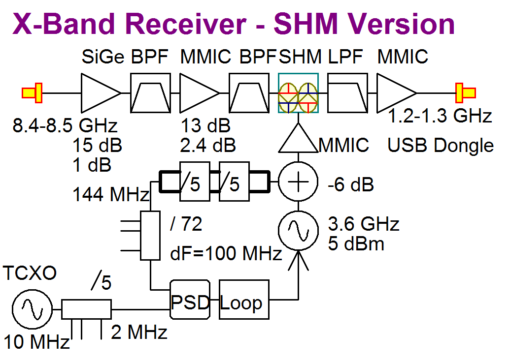
The system diagram shown in Illustration 1 depicts a SHM implementation.
Illustration 1: Architecture based on a SHM
Illustration 1 shows a simple down converter with two cascaded RF LNA, SHM and IF output LNA. The LO required for 8.4-8.5 GHz RF input and 1.2-1.3 GHz IF output is 3.6 GHz (twice this is 7.2 GHz). Many inexpensive divider ICs will operate well at 3.6 GHz but those specified for 7.2 GHz require a third supplier (potentially Hittite). The SHM approach is convenient and allows /5 ICs (or /4) to be used, available from Digikey (NZ). Using two dividers produces 144 MHz, easily processed by an integer-N parallel load divider such as the IDT674-01. This will be divided by 72 producing an output frequency at 2 MHz.
Given this high reference, a simple XOR gate might be suitable as a phase sensitive detector (PSD). This will produce an output a 4 MHz with a duty cycle proportional to the phase difference between XOR inputs and can be filtered by a loop filter. Unfortunately this approach has a limited frequency capture range and produces high reference side-band energy. Consequently, standard phase-frequency detectors (PFD) are preferred. Inexpensive examples include ICS673-01 (IDT), 74HC7046AD (NXP) and HEF4046B (NXP).
The total division effective ratio is /2 /5 /5 = 50:1. Since the reference frequencies is f = 2 MHz, the parallel divider will produce 100 MHz integer frequency steps. In this concept, the IF receiver will provide fine tuning inside this 100 MHz window.
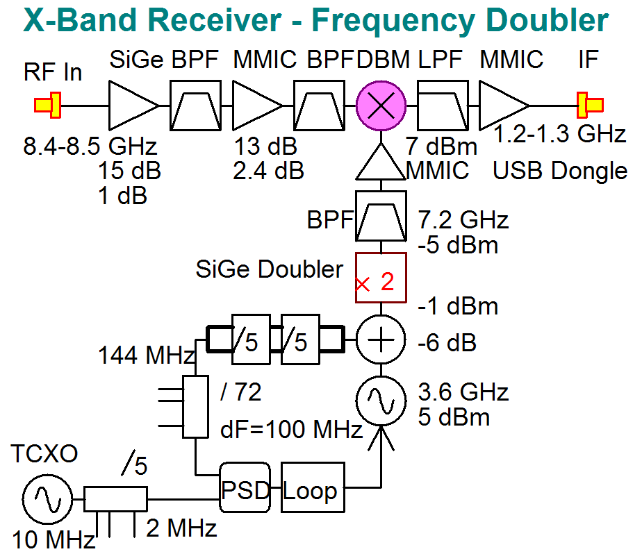
The alternative approach is to use a standard double balanced mixer (DBM) such as those provided by Minicircuits or an interesting SO-8 version from Digikey NZ. These require an LO at f=7.2 GHz, exceeding the capability of dividers readily available from Digikey (NZ). The solution is to retain the same VCO at f=3.6 GHz and follow this with a frequency doubler as shown in Illustration 2.
Illustration 2: Receiver based on LO frequency doubling
Both systems are functionally equivalent. The SHM approach requires circuit level design for its mixer whilst the second requires circuit level design for a frequency doubler. This later approach is slightly more complex, requiring a 7.2 GHz LO MMIC amplifier.
For any design requirement there is usually several suitable options. Some are great in some areas whereas alternatives may be great in others. This is why it is a good discipline to start any design with a list of “drivers” as this will help navigate architectural selection.
Summary
Hopefully this article provides illuminates design methodologies suitable for X-band receiver architectures. These use a single down-conversion followed by a 1.2-1.3 GHz IF. This can either be a commercial receiver, microwave USB dongle or a subsequent second IF design using RF-IQ down conversion to 2-channel audio suitable for a sound-card.
There is no “optimum design” except those that best comply with initial design drivers. If different drivers are defined, alternative implementations may become “optimum”. It is wise to identify what parameters matter most before engaging in any design as this discipline will assist subsequent architectural selection.
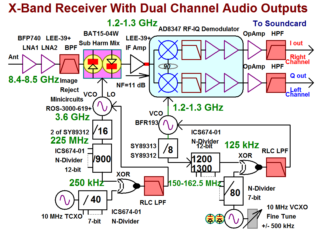
The eventual two-stage superhet from Part 1 is shown in Illustration 3.
Illustration 3: Complete system described in Part 1
The frequency plan shown in this article is slightly different to that described in this article. Also the XOR gate, used as a PSD will be replaced with a conventional PFD IC as this will avoid limited frequency capture range problems. These options show that many approaches are usually available, each performing similarly.
Future Articles
I plan to show circuit topologies for the RF frequency conversion stages in Part 3. These include SiGe bipolar LNA1, MMIC LNA 2, SHM and IF MMIC. Frequency synthesis circuits are planned for Part 4. These include LO MMIC, VCO module, two pre-scaler ICs, parallel N divider, phase sensitive detector and loop filter. Since the topics relevant to each sub system are very different, discussing each in separate articles is appropriate.


